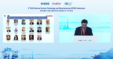
Figure 1 Opening Ceremony of EDTM 2021
The IEEE Electron Devices Technology and Manufacturing (EDTM) Conference is one of the leading conference created by IEEE Electron Devices Society (EDS) to address both the technology advances in micro/nano-electronics and the globalization of the semiconductor industry. EDTM rotates among the hot-hubs of semiconductor manufacturing in Asia. EDTM launched in 2017 in Toyama, Japan, EDTM was subsequently held in Kobe, Japan, in 2018, in Singapore in 2019, and in Penang, Malaysia, in 2020. EDTM 2021 was originally expected to be held in Chengdu China, but due to COVID-19, it has been changed to an online conference.
In addition to ~100 invited talks, there were about 264 accepted papers presented in EDTM 2021, of which 146 papers were presented in oral and 118 papers were presented in poster presentation. All contributed papers went through an identical peer-review process; finally, accepted papers were published in the Conference Proceedings, available electronically on IEEE Xplore.
My research work titled “Effect of Low Temperature Annealing on PN Junction Formation Using Si Paste” was accepted for the oral presentation in the Session 33 FR4P1: Advanced Process Technology II of the conference.
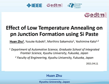
Figure 2 Screenshot of my oral presentation
In this research, low temperature annealing combined with aluminum induced crystallization (AIC) technology are employed to suppress the oxidation as well as achieve a desirable crystallization condition of Si films during annealing process even at low temperature, typically at 600°C or even less. Therefore, the temperature of thermal treatment will be set from 400 to 550°C, the duration will be considered to be several hours to ensure the AIC process. As a result, low temperature annealing technology effectively reduce the oxidation, and the Si paste device using Al substrate annealed at 400°C showed the highest rectification ratio of 3200 at ±1 V, and the lowest reverse current density of 1.8×10⁻⁹ A/cm2. A slight photovoltaic performance was also confirmed by the Si paste device under AM1.5 illumination.
At the oral presentation, various researchers got interested in. I hope that my research work can led to further application of our Si paste in the electronic industry.
At the beginning, I would like to express my heartfelt thanks to the Marubun Foundation for their great support. Participating in this international conference is an excellent experience of strong academic atmosphere for me. I can not only present our current research achievements to famous scholars around the world, but also get valuable suggestions for future research works.
Furthermore, I have learned from the other experts themselves about how to make a professional presentations, and seen the latest findings in the field related to our research and other semiconductor fields, such as graphene device, 2D materials, CMOS device, and so on so forth.
Lastly, my paper was selected as the Finalist for the IEEE EDTM2021 Best Student Paper Award among hundreds of candidates. Though I didn't get to be one of the final three winners, it was still a rich experience for me. It will inspires me to be a top researcher in the future.
