The 5th Nano Today conference is an international conference that aims to assemble researchers that are interested in nanoscience and nanotechnology. It was held on December 6-10, 2017 at Waikoloa Beach Marriott, Hawaii, USA. This conference was organized by the Institute of Bioengineering and Nanotechnology (IBN), as well as by the two premiere journals in nanotechnology, Nano Today and Materials Today. There were 23 oral sessions and 8 poster sessions, which include Synthesis and Self-Assembly of Nanomaterials, Functionalization and Size-dependent Properties, Nanomaterials for Chemical and Catalytic Applications, and Nanosystems for Energy and Environmental Applications, among many others. Over 450 delegates from 57 countries attended the five-day conference. My presentation was included in Poster Session 1: Functionalization and Size-Dependent Properties.
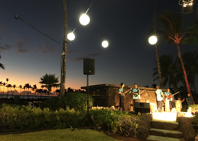
Fig. 1. Waikoloa Beach, Hawaii
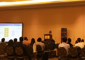
ig. 2. Nano Today Plenary Session
Bimetal-catalyzed formation of InGaZnO nanowires from amorphous thin film
InGaZnO nanowires has shown superior thermal and electrical properties owing to its increased surface area to volume ratio and highly arranged crystal structure [1]. However, only few investigations have been devoted to producing InGaZnO nanowires, since research has been mainly focused on amorphous thin films. In addition, these few studies employed extremely high temperature processing techniques (>1400°C) or contamination-prone solution processes [2-3]. In this study, high aspect ratio InGaZnO nanowires were grown directly from amorphous InGaZnO thin film at 700°C using Mo and Au as metal catalysts. Amorphous InGaZnO thin films (200 nm) were deposited on pre-cleaned Si substrates (1cm x 1cm) via RF magnetron sputtering using sintered (In:Ga:Zn ~2:2:1) targets at room temperature. Subsequently, Mo (100 nm) and Au (2 nm) thin films were deposited using Electron Beam Evaporation. Finally, annealing was performed at 700°C for 2h under N2 atmosphere.
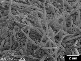
Fig. 3. SEM image of InGaZnO nanowires.
Shown in Fig. 3 is the SEM image of the InGaZnO nanowires. Their diamaters were about 100 to 200 nm, while their lengths were about 3 to 8 µm. This nanowire growth is possibly a synergistic effect of the metal catalytic activities brought about by both Mo and Au. Mo is known to induce crystallization of amorphous semiconductors at a lower temperature than their crystallization temperature [4], while Au has been widely used as a nanowire growth catalyst [1]. The nanowires were also proven to be composed of In, Ga, Zn and O based on EELS mapping. Both Mo and Au were not detected in the nanowire body, which verifies their role as purely catalytic. The single crystalline nature of the nanowires was also confirmed based on TEM analysis and SAED pattern. This technique for growing InGaZnO nanowires from amorphous thin film is a simple, contamination-free and relatively lower temperature process for potential use in future electronic devices.
[1] O. Caballero-Calero, M. Martin-Gonzales, Scripta Materialia 111, 54-57 (2016).
[2] D. Li, G. Wang, Q. Yang, X. Xie, J. Phys. Chem. C 113, 21512-21515 (2009).
[3] Y. Guo, B. Bilzen, J. Locquet, J. Seo, Nanotechnology, 26, 495601 (10 pp) (2015).
[4] Metal Induced Crystallization: Fundamentals and Applications; Wang, Z., Jeurgens, L., Mittemeijer, E., Eds.; CRC Press: Florida (2015).
I am deeply thankful that I was able to attend one of the most prestigious conferences the field of nanoscience and nanotechnology. It was overwhelming to learn about the current trends in terms of applications, and I was able to obtain many ideas that can help me in my own research. I even obtained some useful feedback even after the conference, as I met some professors who are doing a similar study with mine. In my presentation, I got a few questions and comments, as some of the participants found my study simple, interesting and novel. This conference was definitely a great learning experience for me, and at the same time, a once in a lifetime cultural experience in the Big Island of Hawaii. I would like to express my sincere gratitude to my supervisor Prof. Yukiharu Uraoka for the guidance, and Nara Institute of Science and Technology and Marubun Research Promotion Foundation for the financial support.
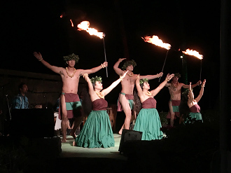
Fig. 4. Hawaiian cultural dance
at the conference banquet.
Fig. 5. Program book and other
souvenirs from the conference.
